
Architecture
Innovative and groundbreaking coherent shared memory technology
The architecture heritage of NumaConnect™ dates back to the development of the IEEE standard 1596, Scalable Coherent Interface  (SCI). SCI was architected upon three major pillars, scalability, global shared address space and cache/memory coherence.
 (SCI). SCI was architected upon three major pillars, scalability, global shared address space and cache/memory coherence.
These principles led to a definition of the packet format with support for a global address space of 64 bits, with 16 bits to address 65 536 physical nodes where each node can hold multiple processors. Each node can then have 256 TeraBytes of memory adding up to a maximum system addressing capacity of 16 ExaBytes (2**64). In that respect, the architects had foresight to envision systems in the exascale range.
The big differentiator for NumaConnect compared to other high-speed interconnect technologies is the shared memory and cache coherency mechanisms. These features allow programs to access any memory location and any memory mapped I/O device in a multiprocessor system with a high degree of efficiency.
It provides scalable servers with a unified programming model that stays the same from the small multi-core machines used in laptops and desktops to the largest imaginable single system image machines that may contain more than thousand processor cores and many Terabytes memory. This architecture is classified as ccNuma or just Numa.
There are a number of pros for shared memory machines that lead experts to hold the architecture as the holy grail of computing compared to clusters:
Any processor can access any data location through direct load and store operations – easier programming, less code to write and debug
Compilers can automatically exploit loop level parallelism – higher efficiency with less human effort
System administration relates to a unified system as opposed to a large number of separate images in a cluster – less effort to maintain
Resources can be mapped and used by any processor in the system – optimal use of resources in a single image operating system environment
No need to decompose or duplicate data sets for scaling – significantly shorter development time for applications like Scale-up and Scale-out for graph processing
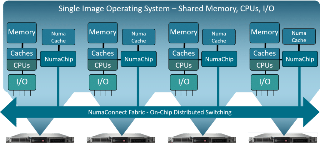 are 64-bytes entities which fits with all modern processor architectures. The link-layer protocol supports a format with little overhead and with flexibility to use packets of 64 bytes for cache coherent transactions or 256 bytes for block transfers. This ensures high efficiency with respect to overhead and fairness for forward progress for all transactions. Scalability is ensured through a distributed, directory-based cache coherence protocol that efficiently reduces the amount of coherency (snoop) traffic that must traverse the interconnect fabric. The directory is implemented with pointers to nodes that share data for any particular cache line and maps the entire system memory. The interconnect fabric can be configured in different topologies by the use of routing tables. The number of fabric channels is implemented according to the customer requirements. The first implementation of NumaChip™ supported 6 x 4-lane channels to accommodate 3-D Torus topologies. The current NumaChip-3 implements 8 x 8-lane channels to support 8 inter-node links. One of the links is implemented as an expansion link to support up to 16-nodes with 32 CPU sockets. The links run at 25Gbps and supports the full Intel UPI 1.0 bandwidth between nodes.